In-Sight 7800 Vision Systems
Full-featured vision system in a flexible, field customizable design.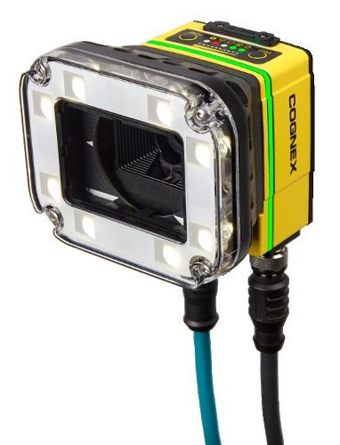
Description
The In-Sight 7800 series is a full-featured, powerful vision system that performs fast, accurate inspections of a wide range of parts across all industries. With a wide selection of field-changeable and user-configurable lighting and optics (Flexible Image Technology™ FIT™) the modular design is highly field-customizable to your application requirements. The In-Sight 7000 vision system is thoughtfully engineered with the full suite of powerful Cognex vision algorithms and convenient features to help you solve your applications easily and reliably, including a highly visible pass/fail LED indicator light ring around the camera body, an SD-card slot and an IP67-rated housing.
- Machine vision system
- Vision System
- smart camera
- machine vision
Product characteristics
- Relative Processing Speed
- 1X
- Resolution
- 800x600640x480
- Frame Rate
- 217/165 (monochrome)135/100 (color)
- Tools
- Blob, Edge, Flaw Detec, Histogram, ID, InspectEdge, OCR/OCV, Pattern, PatMax, Geometry + Calibration
- Tool Options
- PatMax RedLine
- Software Interface
- In-Sight Explorer Spreadsheet and EasyBuilder Interface
Videos
Similar products
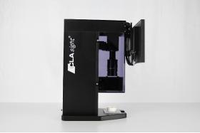
CLA CLINICAL LABORATORY AUTOMATION SA
Switzerland

To meet the growing and increasingly complex demand for machine vision systems, CLA has developed the CLAsight® solution. It is a package consisting of hardware (frame, camera, optics, lighting and industrial computer) and a versatile vision software application for positioning, aesthetic or dimensional inspection, time measurement by direct reading of hands, dial and date, and optical character recognition (OCR). Adapted to your needs, it will be the eye of your robot or the controller of your parts. Application example : - OCR Vision system - Reading of the hands of a movement or a watch - Aesthetic inspection - Positioning of microtechnical parts
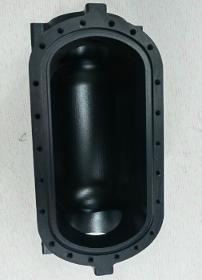
SHENZHEN PROMOSTAR HARDWARE CO.,LTD
Germany
The accessories use for mechanical housing.
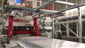
QUELLTECH GMBH
Germany
Particular Challenges of the Application: By tactile equipment, determination of the deepest point on a rough metal surface is neither simple or precise. As a consequence, often either too much material is removed, or the surface is still covered with defects which have to be eliminated by a following milling cycle. The equipment is arranged in parallel, so that the complete width of the slabs is covered. The sensors are calibrated to a common coordinate system and mounted on a movable gantry. Before measurement, the slabs are fixed in place. The scanners mounted on the gantry are guided over the measuring object, driven by an electric motor. The point cloud recorded by the four scanners is consolidated in a PC by means of the QuellTech image processing software which calculates the difference between highest and lowest point of the corresponding surface and compensates for possible inclination of the slab (detrending).
KNIGHT OPTICAL (UK) LTD
United Kingdom
Germanium wafers are a semiconductor material & therefore are a smart choice for microelectronics. Due to its unique electric properties, it is widely used for sensors, solar cells and infrared optical applications. The wafers are also great for microelectronics as the space is limited and being available in 500μm or less it makes it perfect to achieve the high quality results required. It’s thermal conductivity makes it a good alternative to silicon. Our stock wafers are produced as thin as 500μm and provide exceptional surface quality. However, we can manufacture to a fully customised specification with a wafer thickness as little as 10 μm. Typical specifications of our germanium wafers are: 10mm – 150mm in diameter <500μm in thickness Doped and undoped Germanium
Request for quotes
Create one request and get multiple quotes form verified suppliers.
- Only relevant suppliers
- Data privacy compliant
- 100% free