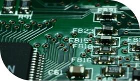
PCB Printing
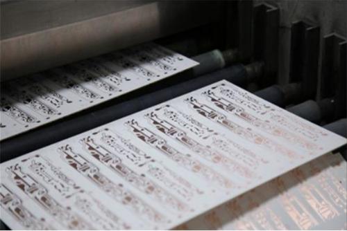
Description
Maintaining a dust-free environment is one of our top priorities, as it eliminates the possibility of any errors that may occur during the printing process.
- Screen printing on metal
- double side pcb
- pcb
- printed circuit board
Manufacturer/ Producer
34071 Istanbul - Turkey
Similar products
XIAMEN NINESUN IMP. & EXP. CO., LTD
China

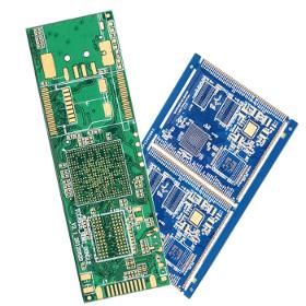
Place of Origin: China Base Material: FR-4 Copper Thickness: 1/2OZ 1OZ 2OZ 3OZ Board Thickness: 0.8mm Min. Hole Size: 0.1mm Min. Line Width: 0.065mm Min. Line Spacing: 0.065mm Surface Finishing: HASL Application: Electronics Device Type: Customizable Solder mask: Black Material: FR4 CEM1 CEM3 height TG Color: Red Blue Green Black Testing Service: 100% Supply Ability: 25000 Square Meter/Square Meters per Month
BERATRONIC GMBH
Germany
Technical data •Max. Panel size up to 1500mm x 670mm •PCB thickness from 0.1-17.5mm •Smallest hole 0.075mm •Smallest trace/spacing 50µm •Copper layer up to 1000µm •Number of layers up to 58 •Aspect Ratio 20:1 •Rigid flex and flex •Viaplugging •Impedance control •Laser Microvias •Blind, Buried Vias Basic material •FR4, FR4 High TG, FR4 •halogen-free, CEM1/3, Rogers, •Ceramic (Al2O3), polyimide and others Surface •HAL lead-free, HAL Pb/Sn, chem. Ni/Au (ENIG), chem. Ni/Pd/Au (ENEPIG), chem. Sn, chem. Ag, OSP(Entek), galv. Ni/Au, Carbon, Ag/Pt (thick film technology) and others Solder resist and placement printing •Different paint systems (including halogen-free) and colors Standards •ISO 9001:2015 / IATF 16949 •UL listing •RoHS / REACH •Manufacturing according to IPC A600 class 2 and 3 Delivery times •Rush service from 1 AT •Series from 10 AT Data preparation •Legacy document preparation •Scan Service •Data conversion •CAM data preparation •CAD layout service
MARXAM PROJECT
Poland
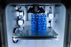
3D product printing technology has gained great popularity in recent years due to its speed, accuracy and economy of manufacturing products. Thanks to the introduction of 3D print to our company, we are able to produce any prototype or serial element. 3D printing services enable the production of both plastic and metal elements in a shorter time than conventional manufacturing methods. 3D printing technologies are characterized by speed and economy, as well as a wide range of applications. We offer 3D resin printing and 3D plastic printing – materials that are used in industry. 3D printing as a service is great for creating prototypes – both in terms of price and execution time. In recent years, this technology has gained much popularity and more and more customers are looking for professional 3D printing services in resistant plastics or in a resin known for its flexibility. Check our offer and 3D prototyping.
DAMEKS
Poland
PCB depanelization is a process step in the production of large-scale assembly of electronics. To increase the throughput of printed circuit board (PCB) and surface mount (SMT) production lines, printed circuit boards are often designed to consist of many smaller individual printed circuit boards that will be used in the final product. This PCB cluster is called a panel or multi-block. The large panel is broken or "depanellated" as a process step - depending on the product, this can be right after the SMT process, after the in-circuit test (ICT), after soldering through-hole components, and even just before the final assembly of the PCBA in the enclosure.
Request for quotes
Create one request and get multiple quotes form verified suppliers.
- Only relevant suppliers
- Data privacy compliant
- 100% free