
BERATRONIC GMBH
Germany

Technical data •Max. Panel size up to 1500mm x 670mm •PCB thickness from 0.1-17.5mm •Smallest hole 0.075mm •Smallest trace/spacing 50µm •Copper layer up to 1000µm •Number of layers up to 58 •Aspect Ratio 20:1 •Rigid flex and flex •Viaplugging •Impedance control •Laser Microvias •Blind, Buried Vias Basic material •FR4, FR4 High TG, FR4 •halogen-free, CEM1/3, Rogers, •Ceramic (Al2O3), polyimide and others Surface •HAL lead-free, HAL Pb/Sn, chem. Ni/Au (ENIG), chem. Ni/Pd/Au (ENEPIG), chem. Sn, chem. Ag, OSP(Entek), galv. Ni/Au, Carbon, Ag/Pt (thick film technology) and others Solder resist and placement printing •Different paint systems (including halogen-free) and colors Standards •ISO 9001:2015 / IATF 16949 •UL listing •RoHS / REACH •Manufacturing according to IPC A600 class 2 and 3 Delivery times •Rush service from 1 AT •Series from 10 AT Data preparation •Legacy document preparation •Scan Service •Data conversion •CAM data preparation •CAD layout service

SUPPLYIZI MATTRESS COVER PILLOW MEMORY FOAM LINEN BED
Turkey
Maintaining a dust-free environment is one of our top priorities, as it eliminates the possibility of any errors that may occur during the printing process.

SUPPLYIZI MATTRESS COVER PILLOW MEMORY FOAM LINEN BED
Turkey
Our advanced systems ensure a continuous electronic exchange of information with customers over the INTERNET. Thanks to the GENESIS 2000 software, the technical information from the customers is converted into production patterns accurately and quickly, and the films are produced with printers to be used in the production stages.

SUPPLYIZI MATTRESS COVER PILLOW MEMORY FOAM LINEN BED
Turkey
Hot Air Solder Leveling

SUPPLYIZI MATTRESS COVER PILLOW MEMORY FOAM LINEN BED
Turkey
Laser cut stainless steel sieve, phosphorus-bronze, adhesive sieve Plate thicknesses: 80μ, 100μ, 120μ, 150μ, 200μ


SUPPLYIZI MATTRESS COVER PILLOW MEMORY FOAM LINEN BED
Turkey
Due to the fact that punching and cutting processes are performed with molds in single-sided printed circuit board production, our company has established its own mold production facility. Printed circuit information from customers is converted into a format suitable for mold production machines in the CAD/CAM work preparation center and transmitted to the mold center via the local computer network. In this center, necessary mold drawings are made using this information, and molds are produced quickly and precisely on state-of-the-art machines.

SUPPLYIZI MATTRESS COVER PILLOW MEMORY FOAM LINEN BED
Turkey
Organic Surface Coating, which is one of the latest technologies among the surface treatment alternatives offered to the customer, ensures that all elements can be soldered well and a flat surface is obtained for proper adhesion of SMD elements to the printed circuit.

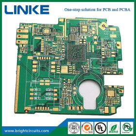
SHIJIAZHUANG LINKE ELECTRONICS TECH CO.,LTD
China
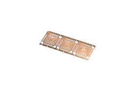
Multilayer PCB circuit board is a kind of printed circuit board composed of alternating conductive pattern layer and insulating material laminated.
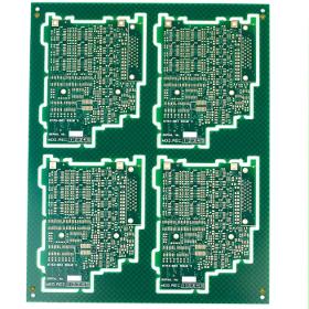
XIAMEN NINESUN IMP. & EXP. CO., LTD
China
Processing Technology: Electrolytic Foil Base Material: Copper Insulation Materials: Epoxy Resin Certification: UL, RoHS, ISO9001, Ts16949 Transport Package: by Vacuum Packing in Cartons Specification: UL, ROHS, SGS Origin:China HS Code: 85340090 Min. Order: 100 Pieces Port: China Production Capacity:100000 Square Meters Per Month Payment Terms: L/C, T/T, D/P Type: Rigid Circuit Board Dielectric:FR-4 Material: Fiberglass Epoxy Application: Consumer Electronics Flame Retardant Properties: V0 Mechanical Rigid: Rigid

DISTRIBUCIONES JULMARSA S.L.
Spain
BASED ON POLYIMIDE FILM COATED WITH A SPECIAL SURFACE CONDUCTIVE ADHESIVE. STATIC GENERATION DURING ROLL UNWIND AND TAPE APPLICATION IS ELIMINATED. IT CAN WITHSTAND WAVE SOLDER TEMPERATURES UP TO 300C AND LEAVES NO ADHESIVE RESIDUE ON PRINTED CIRCUIT BOARDS UPON REMOVAL.
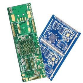
XIAMEN NINESUN IMP. & EXP. CO., LTD
China
Place of Origin: China Base Material: FR-4 Copper Thickness: 1/2OZ 1OZ 2OZ 3OZ Board Thickness: 0.8mm Min. Hole Size: 0.1mm Min. Line Width: 0.065mm Min. Line Spacing: 0.065mm Surface Finishing: HASL Application: Electronics Device Type: Customizable Solder mask: Black Material: FR4 CEM1 CEM3 height TG Color: Red Blue Green Black Testing Service: 100% Supply Ability: 25000 Square Meter/Square Meters per Month

XIAMEN NINESUN IMP. & EXP. CO., LTD
China
Origin: China Model Number: JXFPC Min. Hole Size: 0.20mm Materials: PI/PET Type: FPC Layers: 1-6 Finished surface: OSP/ENIG Board thickness: 0.2mm Solder mask color: orange Certificate: ISO9001 Copper weight: 1 OZ Base Material: PI/PET Copper Thickness: 1/2OZ 1OZ 2OZ 3OZ Board Thickness: 0.20mm Min. Line Width: 0.1mm/4mil Min. Line Spacing: 0.1mm/4mil Surface Finishing: OSP/ENIG Supply Ability: 3000 Square Meter/Square Meters per Month Packaging Details: packing with anti-static red/white bubble Port: Xiamen

BERATRONIC GMBH
Germany
Our services •Layout creation •Material procurement •SMD assembly •Manual and semi-automatic •Mounting •Reflow and wave soldering •Selective soldering •Automatic Optical Inspection (AOI) •X-ray inspection •System assemblies •In circuit tests and •Function test •Revision and repair •Rework Station •Short delivery times
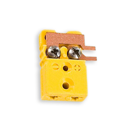
THERMA THERMOFÜHLER GMBH
Germany
Use: Miniature Jack/Socket for thermocouple and RTD circuits. Designed for direct soldering onto printed circuit boards. This version is suitable for flat mounting other versions available, please see separate specification sheet. Mechanical design: • Housing of fibreglass-filled plastic. • Contacts of original thermocouple materials and • spring-loaded sockets for reliable contact. • Moulded barriers prevent short-circuits. • Reverse polarity protection by different contact pin widths. • One-piece housing withstands great stresses.

THERMA THERMOFÜHLER GMBH
Germany
Use: Miniature Jack/Socket for thermocouple and RTD circuits. Designed for direct soldering onto printed circuit boards. This version is suitable for flat mounting other versions available, please see separate specification sheet. Mechanical design: • Housing of fibreglass-filled plastic. • Contacts of original thermocouple materials and spring-loaded sockets for reliable contact. • Reverse polarity protection by different contact pin widths. • One-piece housing withstands great stresses.

Do you sell or make similar products?
Sign up to europages and have your products listed

CRYOSNOW GMBH
Germany
• Optimum handling by compact design • Very low consumption • For difficult to access operations • Small and powerful • No power supply necessary, as driven pneumatically • Maintenance-free • For cleaning injection molds, devices, small components, printed circuit boards, ...
DYMAX EUROPE GMBH
Germany
Dymax Dual-Cure 9014 encapsulant is formulated to cure primarily with UV light and includes a secondary moisture curing function for applications where shadow areas exist on printed circuit boards. Features: - Cures with UV/Visible light - Dual Cure secondary moisture cure capability - Fluoresces blue under black lights - Flexible
SAMSYS GMBH
Germany
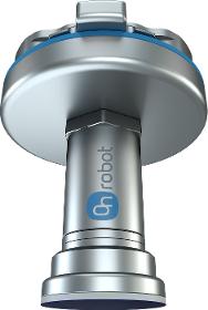
The Gecko Gripper (SP) enables the use of the innovative Gecko adhesive gripper technology in applications with a small surface area. Such areas which could not be automated so far. The gecko-inspired adhesive technology offers precise, track-free gripping. Even with porous workpieces this technology works. For example printed circuit boards or glossy surfaces. Cleaning is not necessary. The three different Gecko Single Pad Grippers (SP1, SP3 and SP5) are named after their payload in kilograms. Of course, the Gecko grippers can be used with leading lightweight robots and cobots. The compact single-pad design allows easy access to the workpiece, even in tight spaces. Since no electronics or air supply is required, the Gecko SP is a cost-effective plug-and-play solution. The Gecko gripper leaves no marks on glass. This eliminates the need for manual cleaning. This means a higher RoI and lower operating costs.

VERPET S.R.O.
Czech Rep.
Preparatory, finishing and other required operations are carried out using bench drills and grinders and other small tools. For example, we provide winding of electric motor components. Polishing and polishing of workpieces. soldering of printed circuit boards, soldering, welding
DR.-ING. MAX SCHLÖTTER GMBH & CO. KG.
Germany
The smallest electronic components, such as chips or connectors, present special challenges for electroplating coatings. In addition to the conductor pattern construction in the manufacturing of printed circuit boards, copper processes are used for filling blind microvias (blind holes) and metallizing through holes. Good metal distribution is necessary even with unfavorable geometry. The most important application areas are found in the automotive industry, telecommunications, and consumer goods industry, but also in the field of e-mobility.

ROVIMEX BATTERY AND ENERGY TECHNOLOGIES
Turkey
100% ozone friendly solvent - meaning zero ODP. Excellent removal of greases, oils and flux residues and acrylic protective coatings from printed circuit boards (PCBs) Leaves a perfectly clean, dry surface – traditional solvents often leave it greasy. It is harmless to most plastics, rubbers, elastomers and surface coatings. NDD is compatible with a wide range of plastics.

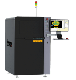
MODUS HIGH-TECH ELECTRONICS GMBH
Germany
The MLD1200 V2.0-OS is a single-sided offline AOI system for the inspection of assembled printed circuit boards from the top. It has one multi-LED illuminated image scanner as well as our patented parallax-free lenses. It includes a modus control unit with the latest modus software. An optional trolley is available. Characteristics: Single system for inspection printed circuit boards from the top side. Combination of different inspection tasks such as SMD placement, THT solder joints, conformal coating and full screening for solder beads (solder balls). Capture of any number of barcodes and data-matrix codes on the multi PCB. Scan range 300 x 400 mm
MODUS HIGH-TECH ELECTRONICS GMBH
Germany
The MLD1200 V2.0-DS is an offline dual AOI system for the inspection of assembled printed circuit boards from both sides at the same time. It has two multi-LED illuminated image scanners as well as our patented parallax-free lenses. It includes modus control units with the latest modus software. An optional Trolley is available. Characteristics: Dual system for double-sided simultaneous inspection for both sides of printed circuit boards. Combination of different inspection tasks such as SMD placement, THT solder joints, conformal coating and full screening for solder beads (solder balls). Capture of any number of barcodes and data-matrix codes on the multi PCB. Shows the test result of both sides at once. Scan range 300 x 400 mm
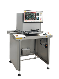
MODUS HIGH-TECH ELECTRONICS GMBH
Germany
The AOI system is designed for simultaneous inspection of printed circuit boards top and bottom side. It has two multi-LED illuminated scan units with parallax free view. Those systems are also available for single side as for top or bottom view. The system includes complete set of modus control units. The transport module has a length of 1200mm (47.2 in). Characteristics: Double System for dual side simultaneous inspection for printed circuit boards. Simultaneous display of all results of double side inspection. Combination of different inspection tasks such as SMD placement, THT solder joints, conformal coating and full screening for solder beads. Capture of any number of barcodes and data-matrix codes on the multi PCB. Scan range 420 x 530 mm or 300 x 400 mm.
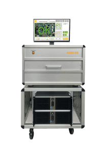
MODUS HIGH-TECH ELECTRONICS GMBH
Germany
The almost maintenance-free modusAOI MCS18/42-Inline was specially developed for transport conveyor modules in production lines. Existing lines can easily be retrofifitted with this system. The small, cost effective system comes with a 18 or 42 megapixels camera, control unit, modus software and led lighting inclusive controller. Characteristics: Single system for inspection of printed circuit boards from the top side. Combination of diverse application tasks such as SMD placement, pre-reflow, chip control, THT fitting, conformal coating and full screening for lost components. Reads barcodes and data-matrix codes in any position and quantity even on multi-PCBs.

OEN CHEMICALS GMBH
Austria
Sodium Persulfate is an inorganic compound. It is a very useful chemical compound which is made by the electrolytic oxidation of sodium hydrogen sulfate. Its chemical formula is Na2S2O8. Chemical Appearance Sodium Persulfate has the appearance of a white crystalline solid. It is almost non hygroscopic. Chemical Applications and Strengths Sodium Persulfate is an extremely useful chemical compound and therefore, has many industrial applications. Its main applications and strengths are: Sodium Persulfate is most commonly used as a radical initiator for emulsion polymerisation reactions for styrene based polymers such as acrylonitrile butadiene styrene. It is used for fast paced curing of low formaldehyde adhesives. Sodium Persulfate itself is a bleach specifically in hair cosmetics and as a detergent component. It is used as a replacement of ammonium persulfate in etching mixtures for zinc and printed circuit boards.

XIAMEN INNOVACERA ADVANCED MATERIALS CO., LTD
China
DBC ceramic substrate: Direct bonded copper (DBC) substrates are commonly used in power modules, because of their very good thermal conductivity. They are composed of a ceramic tile (commonly alumina) with a sheet of copper bonded to one or both sides by a high-temperature oxidation process (the copper and substrate are heated to a carefully controlled temperature in an atmosphere of nitrogen containing about 30 ppm of oxygen; under these conditions, a copper-oxygen eutectic forms which bonds successfully both to copper and the oxides used as substrates). The top copper layer can be preformed prior to firing or chemically etched using printed circuit board technology to form an electrical circuit, while the bottom copper layer is usually kept plain. The substrate is attached to a heat spreader by soldering the bottom copper layer to it. 1. Thickness of substrate can be thin: 0.25mm,0.28mm,0.45mm,0.5mm,0.635mm,1.0mm,1.5mm, 1.8mm,2.0mm 2.
Results for
Printed circuit board - Import exportNumber of results
111 ProductsCountries
Category
- Control boxes - electric (28)
- Printed circuits (16)
- Screen printing on metal (8)
- Connectors, electronic (5)
- Moulding, rubber - machinery (5)
- Monitors, computer (4)
- Measurement - Equipment & Instruments (3)
- Building hand tools, non-power (2)
- Chemicals - Basic Products & Derivatives (2)
- Electrical & Electronic Components (2)
- Electronics - import-export (2)
- Import-export - chemicals and pharmaceuticals (2)
- Integrated and hybrid circuits (2)
- Ovens, kilns, furnaces and hearths, industrial (2)
- Passive electronic components and printed circuits (2)
- Storage equipment and systems (2)
- Abrasives, chemical (1)
- Automation - systems and equipment (1)
- Bar codes - printing machines (1)
- Binding - machinery and equipment (1)