SHENZHEN S&D ELECTRONIC LIMITED
China
Manufacturer/ Producer
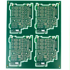
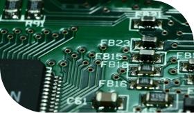
Shenzhen Shen Da(S&D) Electronic Limited was established in Shenzhen city,mainland China in 2002 and is a leading PCB manufacturer which specialise in quick turn, prototype and small to middle volume PCB production. S&D owns 8000 square meters production area, with more than 400 workers, throughput 3000 square meters per month, we manufacture a broad range of PCB from simple single sided board up to 30 layers, Hi-TG, Heavy copper PCB, High frequency, High density, 、Metal base PCB、Flexible PCB , Aluminium PCB. Our products are used in a wide variety of R&D, Consumer Electronics, Telecommunication, Medicals Instruments, Computer, Aviation, Industrial Control, Military area etc. and 80% of our products are exported to Europe, America and Asia. We are a UL, ISO9001: 2000, ISO14001 approved company and manufacture all our PCB by the highest standard. There are a group of skillful workers, professional technical engineers and management teams in our company.
Website
Manufacturer/ Producer
Building A,baishisha Industrial Zone,heping Village,fuyong Town, Baoan District, Shenzhen City, China
518000 Shenzhen - China
Company info
Key figures
-
- Company headcount
- 201 – 500
-
- Sales staff
- 11 – 50
-
- % of export sales
- 80%
Organisation
-
- Year established
- 2002
-
- pages.epage-home.site-status
- Registered office
-
- Main activity
- Manufacturer/ Producer
Business info
Trading areas
- National
- European
- International
Payment methods
- Credit card - Cash - Cheque
- International money order
- Mail transfer
- Swift transfer
- Stand-by letter of credit
- Cash on delivery
- Documentary remittance
- Documentary credit
Banks
- HSBC Hong Kong
Delivery areas
Terms of delivery (incoterms)
- Purchaser
- Shared
- Vendor
Activities of SHENZHEN S&D ELECTRONIC LIMITED
- Printed circuits
- Leiterplatten
europages also recommends
A selection of companies related to the activity:
A selection of products that might interest you
XIAMEN NINESUN IMP. & EXP. CO., LTD
China

Processing Technology: Electrolytic Foil Base Material: Copper Insulation Materials: Epoxy Resin Certification: UL, RoHS, ISO9001, Ts16949 Transport Package: by Vacuum Packing in Cartons Specification: UL, ROHS, SGS Origin:China HS Code: 85340090 Min. Order: 100 Pieces Port: China Production Capacity:100000 Square Meters Per Month Payment Terms: L/C, T/T, D/P Type: Rigid Circuit Board Dielectric:FR-4 Material: Fiberglass Epoxy Application: Consumer Electronics Flame Retardant Properties: V0 Mechanical Rigid: Rigid
BERATRONIC GMBH
Germany
Our services •Layout creation •Material procurement •SMD assembly •Manual and semi-automatic •Mounting •Reflow and wave soldering •Selective soldering •Automatic Optical Inspection (AOI) •X-ray inspection •System assemblies •In circuit tests and •Function test •Revision and repair •Rework Station •Short delivery times
BERATRONIC GMBH
Germany
Technical data •Max. Panel size up to 1500mm x 670mm •PCB thickness from 0.1-17.5mm •Smallest hole 0.075mm •Smallest trace/spacing 50µm •Copper layer up to 1000µm •Number of layers up to 58 •Aspect Ratio 20:1 •Rigid flex and flex •Viaplugging •Impedance control •Laser Microvias •Blind, Buried Vias Basic material •FR4, FR4 High TG, FR4 •halogen-free, CEM1/3, Rogers, •Ceramic (Al2O3), polyimide and others Surface •HAL lead-free, HAL Pb/Sn, chem. Ni/Au (ENIG), chem. Ni/Pd/Au (ENEPIG), chem. Sn, chem. Ag, OSP(Entek), galv. Ni/Au, Carbon, Ag/Pt (thick film technology) and others Solder resist and placement printing •Different paint systems (including halogen-free) and colors Standards •ISO 9001:2015 / IATF 16949 •UL listing •RoHS / REACH •Manufacturing according to IPC A600 class 2 and 3 Delivery times •Rush service from 1 AT •Series from 10 AT Data preparation •Legacy document preparation •Scan Service •Data conversion •CAM data preparation •CAD layout service
DAMEKS
Poland
PCB depanelization is a process step in the production of large-scale assembly of electronics. To increase the throughput of printed circuit board (PCB) and surface mount (SMT) production lines, printed circuit boards are often designed to consist of many smaller individual printed circuit boards that will be used in the final product. This PCB cluster is called a panel or multi-block. The large panel is broken or "depanellated" as a process step - depending on the product, this can be right after the SMT process, after the in-circuit test (ICT), after soldering through-hole components, and even just before the final assembly of the PCBA in the enclosure.
Request for quotes
Create one request and get multiple quotes form verified suppliers.
- Only relevant suppliers
- Data privacy compliant
- 100% free