SHIJIAZHUANG LINKE ELECTRONICS TECH CO.,LTD
China
Manufacturer/ Producer

SHIJIAZHUANG LINKE ELECTRONICS TECH CO.,LTD
China
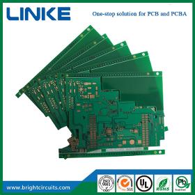
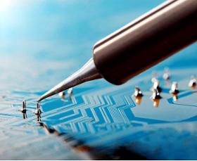
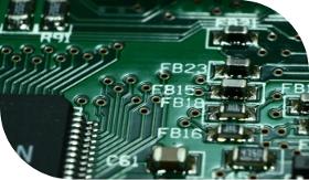
PCB board is also called printed circuit board, it can realize the mutual connection between electronic components. PCB board can be used in different industries of electronic products, it plays an important role. So what are the components of the PCB board? PCB circuit board is composed of: pattern, dielectric, through hole, solder resistant , silk screen and surface Finish.
SHIJIAZHUANG LINKE ELECTRONICS TECH CO.,LTD
China
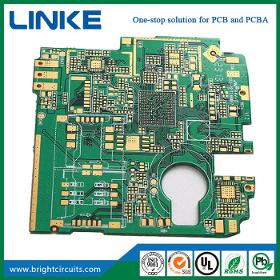
The four-layer PCB board is pressed on the basis of the double-sided PCB board (two-layer PCB board), and PP and copper foil are added to both sides of the double-sided PCB board when pressed, and then pressed into a 4 layers PCB board after high temperature and high pressure. To put it simply, the four-layer PCB board has an inner layer. In terms of process, some circuits are etched onto the inner layer and then pressed.
SHIJIAZHUANG LINKE ELECTRONICS TECH CO.,LTD
China
Multilayer PCB circuit board is a kind of printed circuit board composed of alternating conductive pattern layer and insulating material laminated.

SHIJIAZHUANG LINKE ELECTRONICS TECH CO.,LTD
China
Simply put, Immersion Gold PCB uses a chemical deposition method to produce a layer of metal plating on the surface of the circuit board through chemical redox reactions.
SHIJIAZHUANG LINKE ELECTRONICS TECH CO.,LTD
China
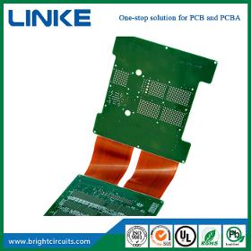
The rigid-flex PCB is a flexible PCB circuit board and a rigid PCB circuit board, which are combined together according to the relevant process requirements through the pressing and other processes to form a circuit board with Flex PCB and Rigid PCB characteristics.

SHIJIAZHUANG LINKE ELECTRONICS TECH CO.,LTD
China
Flexible circuit boards, also known as "flexible boards", are printed circuits made of flexible insulating substrates. Flexible circuits provide excellent electrical performance, can meet the design needs of smaller and higher density installations, and also help reduce assembly processes and enhance reliability.
Manufacturer/ Producer
NO.558,Gongnong Road,Qiaoxi District
050051 Shijiazhuang - China
europages also recommends
A selection of companies related to the activity:
A selection of products that might interest you
XIAMEN NINESUN IMP. & EXP. CO., LTD
China

Processing Technology: Electrolytic Foil Base Material: Copper Insulation Materials: Epoxy Resin Certification: UL, RoHS, ISO9001, Ts16949 Transport Package: by Vacuum Packing in Cartons Specification: UL, ROHS, SGS Origin:China HS Code: 85340090 Min. Order: 100 Pieces Port: China Production Capacity:100000 Square Meters Per Month Payment Terms: L/C, T/T, D/P Type: Rigid Circuit Board Dielectric:FR-4 Material: Fiberglass Epoxy Application: Consumer Electronics Flame Retardant Properties: V0 Mechanical Rigid: Rigid
BERATRONIC GMBH
Germany
Our services •Layout creation •Material procurement •SMD assembly •Manual and semi-automatic •Mounting •Reflow and wave soldering •Selective soldering •Automatic Optical Inspection (AOI) •X-ray inspection •System assemblies •In circuit tests and •Function test •Revision and repair •Rework Station •Short delivery times
BERATRONIC GMBH
Germany
Technical data •Max. Panel size up to 1500mm x 670mm •PCB thickness from 0.1-17.5mm •Smallest hole 0.075mm •Smallest trace/spacing 50µm •Copper layer up to 1000µm •Number of layers up to 58 •Aspect Ratio 20:1 •Rigid flex and flex •Viaplugging •Impedance control •Laser Microvias •Blind, Buried Vias Basic material •FR4, FR4 High TG, FR4 •halogen-free, CEM1/3, Rogers, •Ceramic (Al2O3), polyimide and others Surface •HAL lead-free, HAL Pb/Sn, chem. Ni/Au (ENIG), chem. Ni/Pd/Au (ENEPIG), chem. Sn, chem. Ag, OSP(Entek), galv. Ni/Au, Carbon, Ag/Pt (thick film technology) and others Solder resist and placement printing •Different paint systems (including halogen-free) and colors Standards •ISO 9001:2015 / IATF 16949 •UL listing •RoHS / REACH •Manufacturing according to IPC A600 class 2 and 3 Delivery times •Rush service from 1 AT •Series from 10 AT Data preparation •Legacy document preparation •Scan Service •Data conversion •CAM data preparation •CAD layout service
DAMEKS
Poland
PCB depanelization is a process step in the production of large-scale assembly of electronics. To increase the throughput of printed circuit board (PCB) and surface mount (SMT) production lines, printed circuit boards are often designed to consist of many smaller individual printed circuit boards that will be used in the final product. This PCB cluster is called a panel or multi-block. The large panel is broken or "depanellated" as a process step - depending on the product, this can be right after the SMT process, after the in-circuit test (ICT), after soldering through-hole components, and even just before the final assembly of the PCBA in the enclosure.
Request for quotes
Create one request and get multiple quotes form verified suppliers.
- Only relevant suppliers
- Data privacy compliant
- 100% free